Semiconductor applications
The semiconductor industry can be roughly divided into seven technical fields: semiconductor materials, photomasks, design, manufacturing processes, packaging, testing, and equipment, all of which require vacuum technology as a basis.
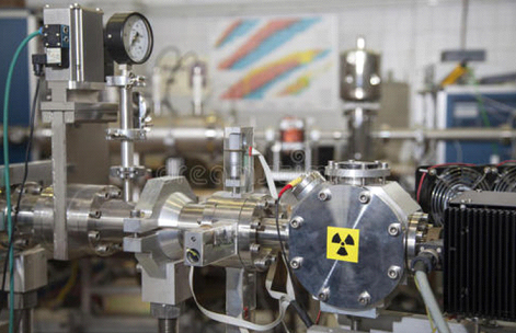
Analytical instruments such as electron microscopes, mass spectrometers, and high-energy accelerators all require a good vacuum environment. Semiconductor technology has entered the age of six-inch, eight-inch, and twelve-inch wafers. To produce ultra-fine metal wires that are almost invisible to the naked eye, strict control and a dust-free environment for semiconductor vacuum systems are required.
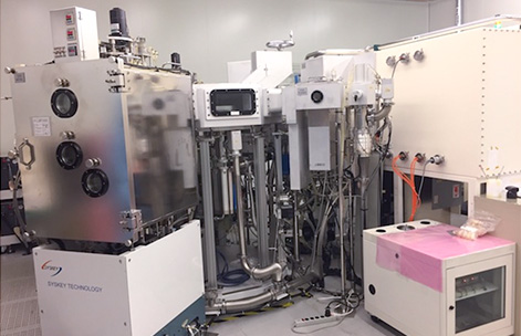
With the development of the information technology industry, the application of semiconductor products has become more and more extensive. Consumer, automotive and communication electronic products have continued to develop, and vacuum technology has also continued to innovate, expanding to include PVD, CVD coating process, electrostatic Equipment such as adsorption disk and etching process has occupied a pivotal position in the advanced semiconductor industry.

